Electrical analysis begins
Now that all these parts have been removed from the inverter unit, we can
start playing with them a bit and explore their electrical/electronic
characteristics. This leads to a deeper understanding of the power
engineering that went into this and current best practice in the field --
possibly to the point of being able to re-use this unit either in another
Prius or as a component of some completely different project. I've spoken
with a couple of colleagues about some fairly scary "Frankenprius" ideas...
Boost coil
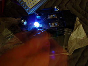
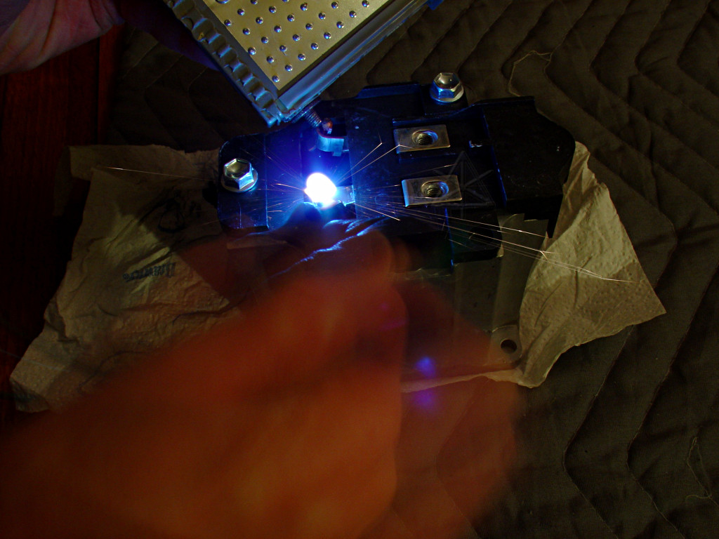
There's not much to the boost inductor. Well, except its ability to store
and release energy! This is a time-shot of quickly brushing past one of its
terminals with a lead from a battery [a Prius module, appropriately enough]
whose other terminal is held on the other coil terminal, and the high-voltage
"pow" and bits of flying molten metal from that single pulse are pretty
impressive. Now, consider that those IGBTs inside the boost switch do this
12,000 times per second and usefully capture all the results! [That figure
is real, from watching the CPWM converter-drive lead from the car's ECU.]
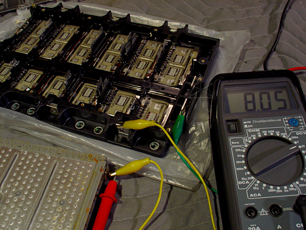
Power transistors
How about those big power transistors? What are their characteristics?
With gates that massive, how much charge does it take to turn them on?
Here we won't get a quantitative idea of that, but a little playing around
can give some idea. The Prius battery module is hooked up to emitter and
collector through a dropping resistor to limit current to about an amp, and
we read the voltage across the transistor. With it off, I see full battery
voltage. [Which, by the way, is normal real-life for a 6-cell Prius module
even though it's rated at 7.2V]
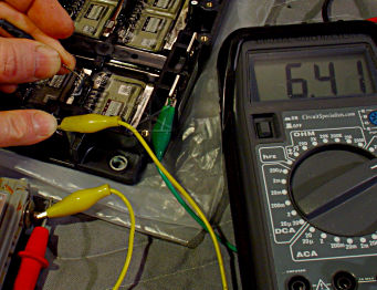
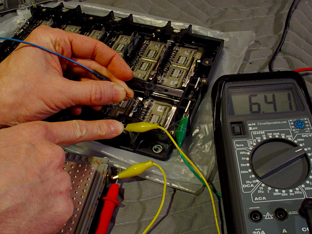
Using a pin-probe, a couple of fingers, and my body as a large resistor,
I can bleed a little charge into the gate lead and watch the voltage across
the transistor decrease as it starts going into conduction. Holding long
enough, i.e. a few seconds depending on how hard I press the metal, clearly
goes all the way into saturation, and then by shifting my other hand to the
negative lead I can drain charge and get it to turn off again. Here, though,
we've gotten a little way into the linear region...
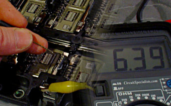
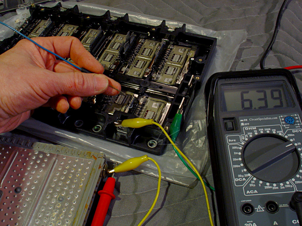
and by removing the pin-probe to the gate, I can cause the voltage to just
freeze right where it is. It just holds there -- doesn't drift up or down
for a very long time, until the charge is given a path to dissipate by
touching the gate again. Just like a FET should, of course, and the leakage
exhibited here is small to nonexistent.
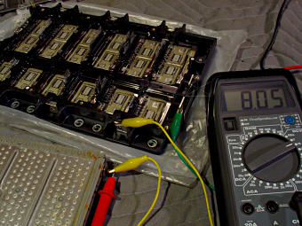
Forward voltages appear to be fairly normal -- diodes and saturated transistors
at 0.6V when non-trivial currents [~120 mA] are passed through them. The
forward voltage of the entire rack's worth of diodes, taken at the supply
inputs, reads 0.95 under the same conditions. You can guess what would happen
if this were hooked up to the 200V battery as ORNL had it labeled! Playing
with higher voltages and currents through the rack will wait until some later
phase of testing.
The devices in the boost switch are similar, although its diodes appear to
have a lower forward voltage of 0.5. Obviously, the lower the better.
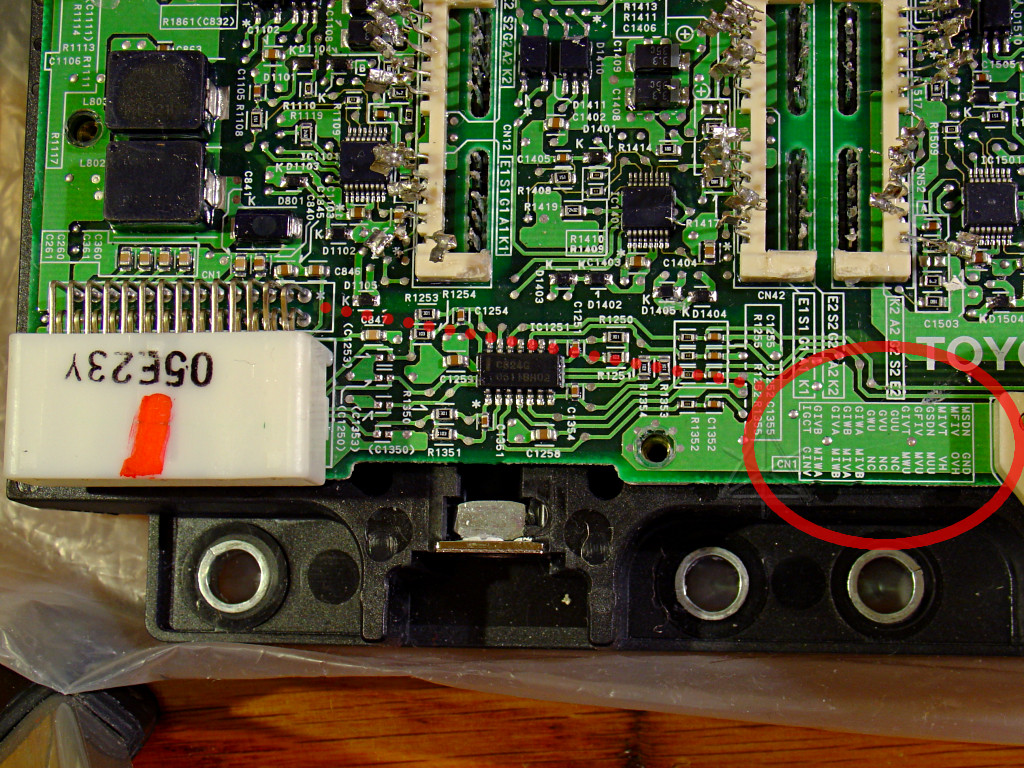
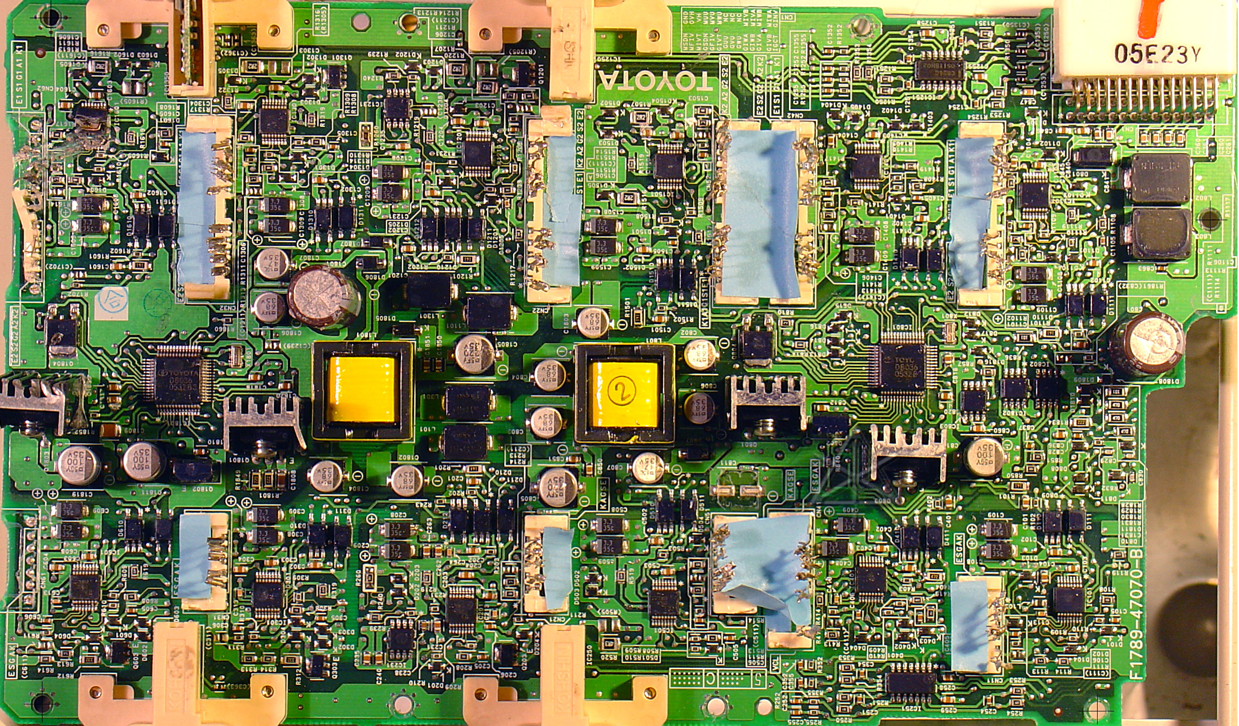
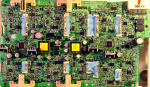
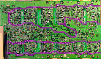
Control board
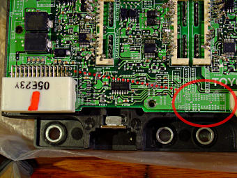
The control board has its interface connector nicely documented, albeit at a
bit of distance. These connection names are the same as used at the ECU, and
described in the "Terminals of ECU" section of the service manual. This is
really useful, because it indicates how to hook it up to power and where to
find real-life signals in the running car to try and reproduce on the bench.
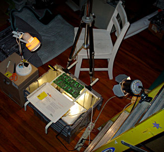
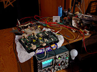
First, we need to get the best possible pictures, not only of both sides of
the board but also attempts to probe *inside* a little by shining light
through to show where the vias are and even which direction they might
roughly head. This was a quick-n-dirty rig to hold the board at the edges
and light from above or below and try to keep the camera exactly positioned
the same way. It almost worked as intended; a bit of post-correction was
definitely necessary.
|
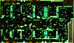
|
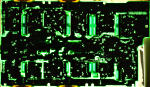
|
|
Front
(front lit)
|
Front
(back lit)
|
Back
(back lit,
flipped R/L)
|
Back
(front lit,
flipped R/L)
|
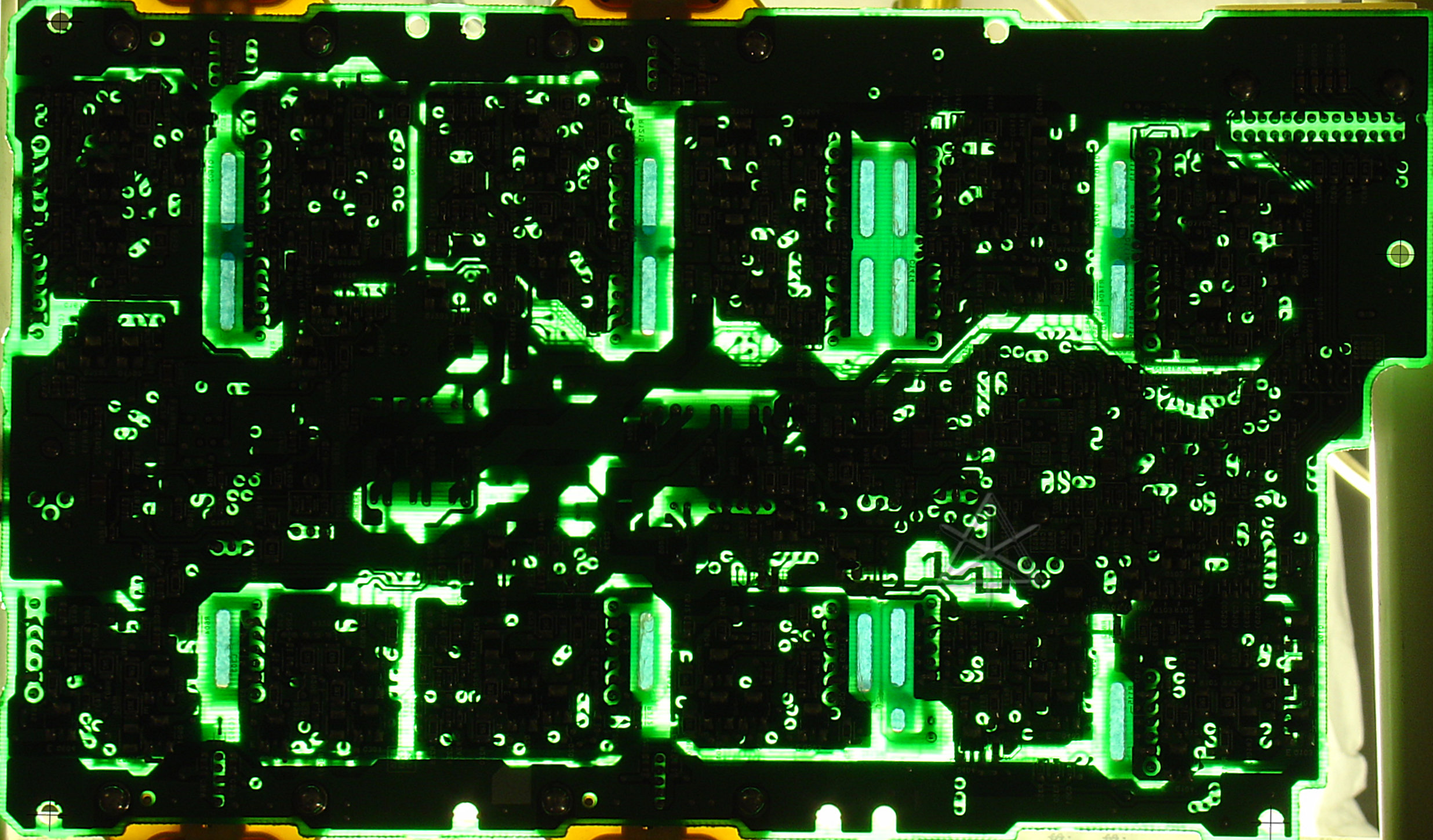
Here's a set of four large images that have been stretched around a little
bit, and the rear-view ones flipped right-to-left, such that they very closely
match up via-for-via when loaded into one's favorite image editor as layers
on top of each other.  There's a lot of power-plane in there, so this may or
may not help with further circuit-tracing but is kept here for reference.
The blue tape over the gate connection slots is simply to keep light from
blasting up through them from underneath.
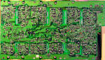
With a little more familiarity with how the thing is laid out and what to
connect to, it's time to get the *good* module on the bench and start tracing
some things.  No IGBT rack connections are needed yet, this is just playing on
the 12V side and trying to figure out what eventually gets sent to the gates.
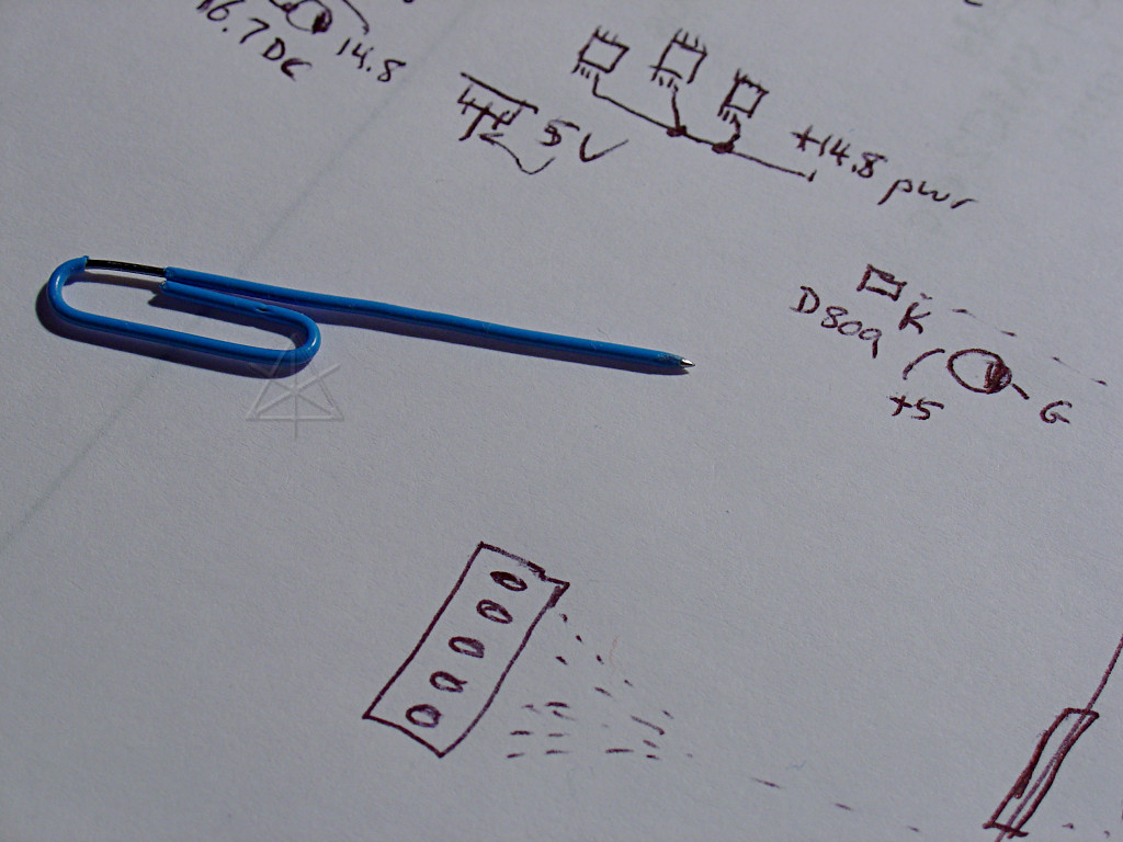
To get through the conformal coating to reach solder lands, a very sharp pin
probe is needed.  It's easy to make one out of a paper clip; the plastic-coated
type provided a little more protection against randomly shorting things if,
say, it's dropped onto the board.
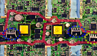
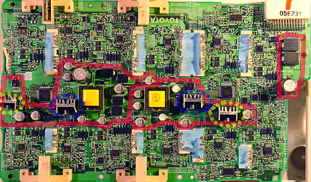
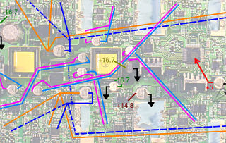
A little bit of 12V conditioning happens over at the right, and then the entire
middle section [red boundary] consists of two mostly independent power
supplies.  Upon supplying 12V power to IGCT and GINV, the two yellow
transformers begin emitting a soft but audible high-frequency hash typical
of switching power supplies, and a whole bunch of voltages appear at the small
electrolytic caps scattered around them.  The two heatsunk power transistors
circled by blue dots are tied to ground at the emitter and exhibit the high-
frequency [and somewhat jittery] transformer-drive waveform, and the ones
circled with yellow dots seem to be linear regulators for 5V that feeds the
two processors and some other stuff.

The board draws about 0.7A at 12.5 volts, and 0.8A at 10 -- higher draw with
less voltage, typical of a switching power supply.  At 7.8 volts it draws about
an amp while trying vainly to start up.  The 5V fails at 5.7 volts input,
indicating fairly low drop-out regulators.  After the board has been running
for a while, the warmest components on it are the little yellow transformers.
And not inordinately so -- once again, high efficiency, minimal wasted power.
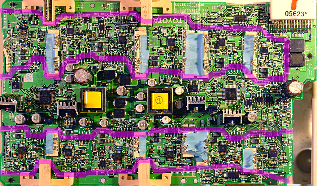
Strict isolation is maintained between the chassis-grounded 12V system and
the entire HV system including battery, motors, and transistor rack.  But the
inverter is one of the places where they must come close together, so there
needs to be a bit of magic here.  [The other place, of course, is in the
battery ECU for sub-pack voltage monitoring.]  There are isolation barriers
down the whole length of the board, bridged by pairs of optoisolators to pass
signals in various directions, and all the power to the gate-driver circuitry
comes from isolated sources.  So that's almost TWO layers of isolation if you
consider the insulated gates another barrier.  Well, you can't really think
of it that way because the high-side gate driver circuitry has to operate
somewhere above the motor lead's voltage at any given time so that whole
section must float around at a fairly high voltage when running.  What's not
yet clear is exactly how that's done, or [related] how the ground-fault
monitoring works.
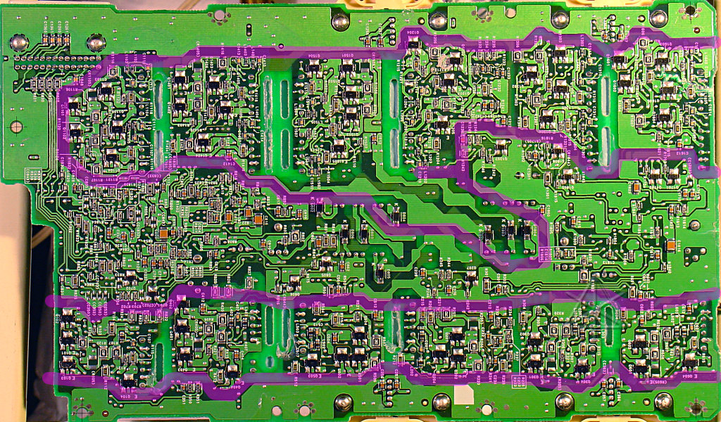
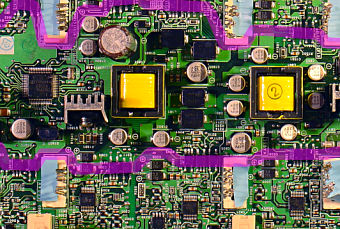
The isolation gap is even more obvious on the backside of the board, but this
also shows how some of the floating power-supply outputs connect to the HV
side.  The upper and lower edges of the board get back into non-isolated
territory, to interface directly with the current-sensors [which are yet
another isolation-barrier component!].  In this view, there are twelve fairly
distinct denser areas of circuitry near the control-lead slots -- these are
the sections that stay isolated and actually control the transistor gates.
With that in mind, a couple of hours of probing around with a scope and meter
in "diode check" mode to find where things are hard-connected together has
pretty much ferreted out where all the power goes. It is soon apparent that
split (+) and (-) supplies are utilized -- they feed several analog components
including the current sensors. Those are interesting -- they appear to have
two exactly duplicate outputs, which get routed back to the interface connector
as signals like "MIVA" and "MIVB" which scope out as exact clones of each other
in the running car. Why two?? Not only that, but they swing above AND BELOW
ground, right into the hybrid ECU. That means the hybrid ECU must have some
negative-supply stuff inside it too. Why not an easy single-supply swing about
2.5V, like the main battery current sensor? A bit of a mystery there.
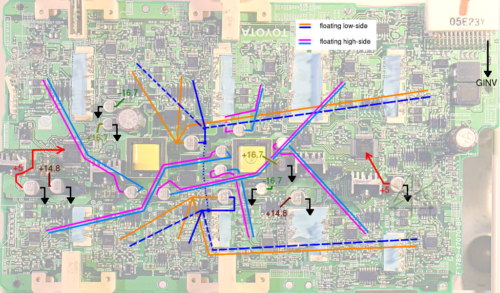
The really fascinating thing is how the gate driver supplies are done. Each
power supply section produces four separate 9.5V or so floating outputs, one
slightly more heavy-duty [well, at least with a larger filter cap] than the
other three. The large one [where "large" simply refers to its capacitor]
feeds all the low-side transistor drivers. The three smaller ones each
independently feed the three high-side driver sections for MG1 and MG2, which
begins to make it clearer how the high-side isolation is done. The answer
seems to be six totally separate little supplies.
In the assembled module, all the low-side supply negatives are hard-tied to
each other, the "E" control leads, and the main (-) supply from the battery.
But there's something a little funky about them -- without the transistor
rack in place, the negatives [blue] of the low-side driver supplies aren't
tied to each other [lightly dotted line] and are only hard-connected to the
driver circuitry in the "V" areas. It isn't clear how the negative supply
for "U" and "W" gets there but there's some other component in the way. But
the three positives per side are definitely tied together as shown. Again,
once this is all soldered down to the rack, it's largely irrelevant and all
rides wherever the negative of the 200V battery sends it. I can also see
that there's an extra optoisolator device from the "V" low-side back into
the nonisolated area, which is undoubtedly related somehow to why it's got
the "real negative".
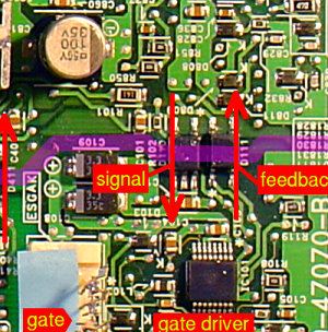
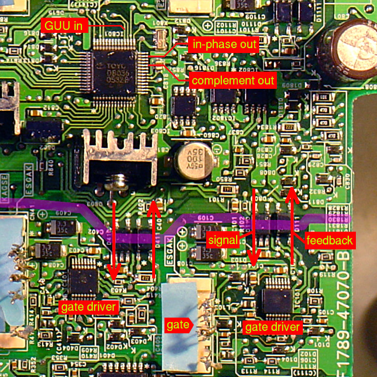
Here are some of the early discoveries as to where the switching signals
go.  I'm sending a simple oscillator into the "GUU" lead, which controls
current to the "U" phase of MG1, and trying to find how it eventually gets
to the IGBT gates.  I've found it up to the processor, which is a dead end
until the "GSDN" gate/shutdown lead is brought high too, and then I discover
a split-out pair of complementary signals in response that eventually hop
through two of the optos and go to the gate driver chips.  When GUU is low,
the lower transistor of the pair is turned on; when GUU goes high, it turns
off and the upper transistor turns on.  There is NO both-off state, except
for when the overall "gate" lead goes low and then all the transistors turn
off [i.e. the definition of "neutral" in the car].

This switching works down to DC and has a little hysteresis, changing state
as the input rises above 8 volts and again as it falls below 6.8 or so.  No
IGBT gate output appears until "xSDN" is brought high, and then the next
rising or falling edge at the "xyU" lead starts producing output.

In the MG2 section, each transistor gate pair is simply tied together, so
the gate driver chips are evidently amply capable of kicking both of those
monsters at once.
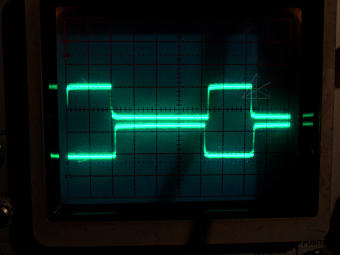
The last thing anyone wants is both elements of a half-bridge to be on at the
same time, which would cause a shoot-through short across the supply and rapid
loss of the magic smoke that makes things work.  Since you can't instantly
turn on one element of a half-bridge and turn off the other and guarantee no
transition leakage, there has to be some minimal amount of guard time during
which both are solidly OFF, usually enforced in hardware.  Here, by sending in
a single squarewave input and scoping the corresponding pair of gates, I've
found that time to be 6 to 8 microseconds.  This appears to be done at the
processor outputs; it isn't yet clear if there's a backup system to prevent
disaster if the processor should ever wig out and turn on both outputs at once.
Given the amount of circuitry around the gates, I would expect an additional
level of protection in there someplace -- but that would mean more signals
needing to cross the isolation boundaries.  Maybe that's part of the feedback
path -- remains to be seen.

For all its sophistication and apparent complexity, this device is still wholly
a slave to the hybrid ECU.  It does exactly what it's told via the gates and
switching-control lead triples, and only sends a little running data back.  It
has no sense of 3-phase sequencing and cannot intelligently drive the motors
for propulsion by itself.

From here, I can try to find some part numbers to help further determine
functionality, compare against what other analyses have already found, and
start getting into what someone would need to know about switching strategy
to usefully control this mess.  And I still haven't even touched the cooked
DC/DC to try and figure out what the heck happened to it yet.
Next: Electrical analysis continues
Home
_H* 070604